These schematics and notes are presented to help you understand how the Tech Edge
2Y2 DIY Wideband unit works.
You will note that although we have made it available as a DIY unit, it is designed to give
results equivalent to professional controllers costing 10 times as much.
This is possible through the careful selection of key performance determining components,
and we have not over-specified parts that are not critical to the unit's performance.
The key component of the design is however the proprietary firmware that is written
in assembler for speed, and this is teamed with a fast 8/16-bit RISC processor that exceeds 10 MIPS
performance, along with a fast 12 bit hardware DAC as used in our top-of-the-range units.
Several years of trouble-free operation of the original 2A0 and 2A1 firmware has proven the basic design in many automotive and industrial applications. Rest assured that many thousand of constructors around the world have successfully constructed this and similar Tech Edge DIY wideband controllers. Please note that all images and text are Copyright © 2012 Tech Edge Pty. Ltd.
2Y2 comes with a black ABS case (grey case shown). |
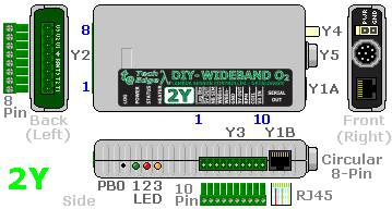
SCHEMATIC INDEX1. Atmel Mega-168 Microcontroller2. Power Supply, H+ & Power Cable 3. WB-Module Connector & Socket Y5 4. User & Thermocouple Inputs 5. Thermocouple Amplifier & Links 6. RPM Capture & Signal Processing 7. Outputs WBLIN +/-, NBSIM & SVOUT 8. TWI &SPI Interface, & Button(s) 9. 1 Megabyte Flash Logger Module A. LEDs & External 5 Volt Power B. RS232 Driver, Splitter, Y1A & Y1B C. Sensor Cables (LSU & UEGO) D. Serial Cable (RS232, WB-PC cable) E. Four Digit 7 Segment Display Option |
In this document, the first time a term is used (and often in subsequent sections), we show part the number (eg. U1) as blue bold, and we show the signal and/or electrical connection name (eg. OC1A) in red bold. If there is a pop-up window that shows additional detail, we show it as a red underlined link (eg. connector Y4). We highlight important information with red italics (eg. Construction note:) and show less critical information in blue italic (eg. nominal value is 47k at 25°C) We show orderable parts in upper-case green enclosed in square brackets (eg. power cable [20PWRCBL] and sometimes even have a link to the order page (eg. power cable: [20PWRCBL]). Lastly, although we have tried to maintain this scheme, you will find paragraphs where we break our own rules!
(1) Atmel Mega-168 (M168) Microcontroller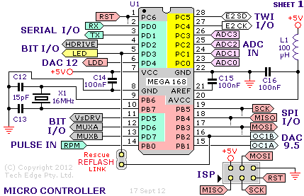
An Atmel Mega-168 (called M168 here) RISC CPU U1 (Microcontroller) provides the unit's intelligence. The M168 in DIP format is a 28 pin device. A couple of analog MUX devices are used to expand the effective number of analog inputs to 16 (one of these muxes is on the lambda module). The M168 has 8k words (= 16k bytes) of 16 bit program memory, 1k byte of internal RAM and 512 bytes of internal EEPROM memory. The M168 family derives from the Atmel Mega-8 (M8), and the M168 has twice the program code space (it is part of a family - the M48, M88, M168 & M328). The TWI interface (also called I2C) and SPI interface (described below) provide fast, low level, serial connection to additional hardware (optional on-board logger-memory, optional LED display, etc.). Other pins drive other hardware devices (eg: heater switch, status LED, PWM outputs, etc.). An internal UART provides RS232 communication for logging and user interface functions. The schematic shows the 16 Mhz crystal X1 (with oscillator load capacitors C12 & C13). CPU power decoupling capacitor C14 (along with regulator filtering described below) reduce noise to the CPU. Analog reference (AREF) decoupling capacitor C15 does the same for the CPU's internal ADC. Inductor L1 along with capacitor C16 filters the CPU's Analog power supply (AVCC). Note the two GND pins - one is beside the AREF pin and is designed specifically to be the analog GND point. In the diagram the CPU's pins are colour coded into like-coloured port groupings B, C & D. Outside the block the coloured pin-name tabs show how functions are grouped. Of special note are the OC1A and OC1B outputs that are designed as PWM DACs with an effective resolution of around 9.5 bits. The DAC12 output also uses the SPI signals (MOSI, MISO & SCK) to interface the CPU to the 12 bit hardware DAC on the lambda module. Other control lines (HDRIVE, VsDRV, MUXA & MUXB) from the BIT-I/O group also go to the lambda module and other points on the main board. Other points to note are that although the 2Y1 did not have an ISP (In-circuit Serial Programming) header), and we thought there were good reasons not to add one, we have added one for the 2Y2 (but the kit does not actually include the 6 pin header pins). We added the ISP interface for possible future expansion (and because we had the space to do it!). Note: the RST (Reset) pin goes only to the ISP header, although it is possible to use this pin as a bit I/O line (with some restrictions). Also note: other lambda controllers we manufacture use are the 32 pin QFP (SMD chip) version of the M168, and this chip has 4 extra pins over the 28 pin DIP chip - two pins are extra GND points, but two are extra ADC channels (ADC6 & ADC7). |
(2) Power Supply, H+, Filtering & Power CableAs well as the +5 Volts generated by 7805 TO220-package regulator U10 that is used by most of the circuitry, the main power supply also provides the unregulated HEAT+ voltage that heats the wideband sensor (HEAT+ is controlled by the pre-built lambda module using PWM switching). 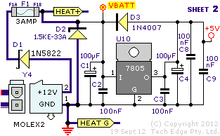
3 Amp fuse F1 (using PCB mount clips F1A & F1B) provides protection against shorting and internally generated fault conditions. Reverse polarity protection is provided by Schottky diode D1, while fast Zener D2 (Tranzorb®) provides transient suppression. The raw unregulated power is called VBATT. Diode D3 protects the regulator from shorts across the battery input where the regulator's output voltage, (supplied by C4) is higher than its input voltage. Capacitors C1 & C4 (electrolytic capacitors), and C2, & C3 (block mono capacitors) filter and suppress electrical noise around the regulator. C8 provides power supply bypass filtering for the thermocouple amplifier, and C9 does the same for the pre-built lambda module - they are described below. 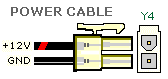
Molex MiniFit-Junior® (connector Y4) connects the unit to the mating power cable shown at right. Note that prebuilt cables have the power conductor with the white flash connected to the GND pin. Red heat shrink positively identifies the battery (+12V) connection (note also that the negative lead has the white tracer!). Prebuilt 2.0 m power cables are available as spare part [20PWRCBL], and Molex connector kits are available as spare part [PWRPLGK]. Note carefully that the 2Y2 controller is designed to operate from a minimum voltage of (approx.) 11.0 Volts (design value of 10.5 Volts plus D1's Schottky voltage drop of up to 0.5 Volt) to a maximum of (approx.) 19.5 Volts. The voltage limits are to protect the sensor from over current damage - the status LED warns of over/under voltage conditions. In operation the regulator U10 does not dissipate much heat and sufficient heat sinking is provided by the main PCB it bolts to. Construction note: U10's M3 mounting bolt also secures one half of the prebuilt lambda module via a spring washer and M3 nylon spacer screwed into the top of this bolt. The identical fuse holders F1A and F1B (make sure each half is oriented correctly) may need minor surgery, in the form of bending the end retaining-tab, when a longer than normal fuse is supplied. |
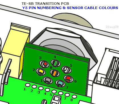
(3) WB Module Connector, Transition PCB & Sensor Socket Y5The 8 pin circular panel mount male socket Y5 (at the end of the case) connects the wideband unit to the sensor cable. Y5 is soldered directly to the small transition PCB (it is labelled TE-SB). The transition PCB is then connected to the main PCB with semi-flexible bare copper wires. Note that the pins on Y5 in the schematic below are shown oriented from outside the case (NOT the solder side). More information on this tricky aspect of construction can be found in the construction manual. Note: in case you missed it - here is a diagram of how Y5 should be mounted to the transition PCB TE-SB. Be warned that constructors have failed to understand this simple diagram, and have spent hours rectifying their mistake! In the diagram, Y5's pins are colour coded according to the sensor cable's colours. 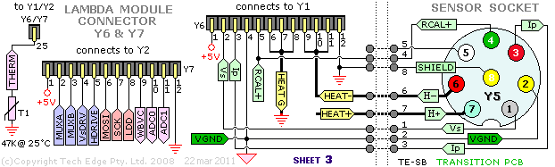
The 2Y2 pre-built lambda module uses a 0.1" spacing header Y6/7 with 25 pins to connect with the main board and the sensor socket Y5. The signals to/from the lambda module are split into two sections that interface directly with the wideband sensor (Y6), and to the microcontroller (Y7). Note that the heater current carried in the HEAT- and HEATG circuits are split between 3 pins each of Y6 to minimise any problems associated with the high current carried through these pins. All other circuits carry only small currents and a single pin therefore suffices. The sensor's HEAT+ signals (also called H+) comes directly from the power supply section described above. The thermistor T1, with nominal resistance of 47k at 25°C, allows the absolute on-board temperature of the 2Y2 unit to be measured. This provide cold junction temperature measurement for software compensation (CJC) for thermocouple readings. Note that T1 is located near the thermocouple connector Y2 as this is the junction temperature that is compensated for. Note that the thermistor is connected to pin-0 of Y7 (Y7p0) and this is behind Y7p1 so that Y7 has an L shaped layout. More information, and schematics, for the lambda module can be found here. The 2Y2 lambda module is the same as the 2Y1 (although one is black and the other green), and both have a wire-wrap link (we forgot to fix for 2Y2!). |
(4) User & Thermocouple Input MuxingThree of six user inputs are set up to sense K-type thermocouple inputs (TC1 to TC3), and three are 0 to 5 Volt analog inputs USR1 to USR3. The three thermocouple inputs can be set up as normal 0-5 Volt inputs . This means six 0-5 volt inputs can be logged in addition to Lambda and RPM.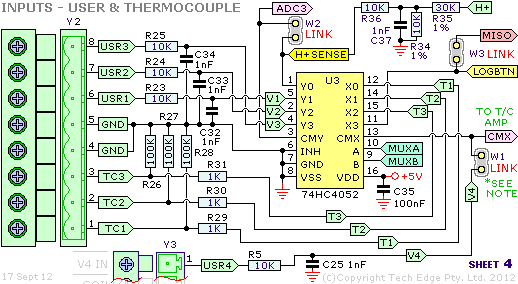
The 8 pin pluggable connector Y2 at the end of the case carries three thermocouple inputs (TC1 to TC3, and three user voltage inputs (USER1 to USER3). Note: this connector is reverse numbered from the right. Additionally, pluggable connector Y3 carries a single user input V4 IN (pin 10, rightmost on Y3) that is also on this circuit. Note: V4IN cannot be accessed with the standard hardware, firmware and normal link settings. V4IN is used only for a cut-down version of the unit (but we still supply the input filtering parts R5 & C25 in the kit!). Because we need more inputs than the microcontroller's 28 pins allows for, a two section four channel multiplexer (MUX = 74HC4052) U3 is used to select 8 lines into two ADC converter inputs. The MUX is controlled by lines MUXA & MUXB and the MUX output CMY goes to processor input ADC3 and MUX CMX output goes to the thermocouple amplifier described in the next section (and then to ADC2). As well as the analog user inputs, The heater positive voltage H+ (see previous section) is divided by 1% resistors R34 & R35, filtered by C37 to give H+SENSE. This voltage is ¼ of the H+ voltage and H+SENSE is also an input into the USER side of the MUX. The thermocouple side of the MUX also senses LOGBTN levels (see here).
Analog user inputs USR1 to USR3 and H+SENSE have a very simple filter comprising 1 nF bypass capacitors and 10 k input resistors. The Thermocouple (and LOGBTN) inputs are filtered by the thermocouple amplifier described below. |
(5) Thermocouple (T/C) Amplifier & Option Links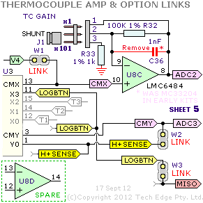
Op-amp U8C amplifies the signal from all thermocouples (and the LOGBTN signal too, see previous section). This amplifier is a compromise, and three individual thermocouple op-amps with (+)ve and (-)ve inputs would have been better (but we only had a certain number of input pins). C36, originally specified as 1 nF, was designed to provide some measure of thermocouple filtering. *In April 2009 we decided to remove this capacitor because, even when made quite small, it stores enough charge that it bleeds this through to the other channels (when in x101 mode) and corrupts their value. Note: software processing also performs filtering of these signals. The gain of the op-amp can be set at either 101 or, for redefining the T/C inputs into 0-5 Volt User inputs, set to 1. But note that ALL the T/C inputs are affected by the gain setting, and individual inputs cannot be selectively redefined like some of our other models. Theory tells us gain is (R32+R33/R33) and with shunt J1 in the x1 position, R32 is shorted so the gain is set to 1, or, when not shorted (ie. J1 in x101 position) gain is 100+1/1 = 101. The 101 gain stage results in a full scale 5.0 Volt input to the M168 at a T/C input voltage of 5000/101 = 49.5 mVolt. This K-Type table shows that 49.5 mV corresponds to 1218 °C for the thermocouple. In theory, changing R32 to a value larger than 100k will increase the gain, and the same thermocouple can be used to cover a lower temperature range (or a different type of thermocouple used), but remember if you do change the gain, that logging or display software must be told of the non-standard settings. Larger values of R32 may also cause gain instability so you may have to provide some signal filtering. CJC: The T/C voltage is actually being measure between the cold junction (in the 2Y2 controller) and the hot junction at the thermocouple itself. To calculate an absolute temperature the temperature of the 2Y's cold junction is measured with thermistor T1 and then this temperature is added to the computed thermocouple's raw temperature. Thermistor T1 (see above) is physically located beside connector Y2. T1 has a nominal resistance of 47k at 25°C and, with a simple calculation (use this excel spreadsheet), can measure absolute temperature of the board. Cold junction compensation (CJC) may be very important if K-type thermocouples are used for low temperatures. For example, for a thermocouple at 500°C, and a case temperature of 50°C, without CJC the measured temperature would be 10% off. Option Links: There are three links on the board W1, W2 & W3. In normal operation none of these links is fitted. It is possible to build a minimal version of the controller by removing all the USER and TC inputs. Further savings can be made by removing MUX chip U3 (described above), but to do this, the W2 link must then route the H+SENSE signal to ADC3. Link W1 can then route the V4 signal to ADC2 (V4 is the processed V4 IN signal from the Y3-pin 10 input. This scheme allows a single user input to be read (it will be duplicated in the logging data stream). Finally the W3 link should normally NOT be connected as the MISO signal is critical to normal operation of the wideband unit, and its function cannot be modified without firmware changes. Note: No firmware changes are required if the above changes are made, and the standard HXF files are used. Updates: Note that U8 was originally specified as an MC33204 but, for better thermocouple operation at room temperature and lower temperatures sensed by a K-type thermocouple, we now use the better LMC6484 chip. *As noted above C36 is removed to enable proper thermocouple operation (ie. for J1 in the x101 position). More info here. Accuracy: Remember that the M168 uses a 10 bit ADC converter (ie. 1024 levels over 1218°C input), and in theory the best resolution is 1218/1024 ≈ 1.2°C. In reality, without software averaging, one can expect at least 8 bits (256 different levels) of accuracy for the ADC, and this results in about 4°C (≈7°F) resolution. Software averaging can improve this figure, but it demonstrates the absolute accuracy, and limitations, of the T/C inputs used on 2Y. |
(6) RPM Capture & Signal ProcessingThe M168 has a number of useful hardware modules. A 16 bit hardware counter is used to process time intervals with a 5 µSec. resolution. The CPU's PB0 (ICP1) pin has an input capture function and this pin is driven by the RPM signal from the circuit shown here. Two input levels are available; a higher voltage designed to connect to the COIL primary of a conventional points ignition system, and a lower level input designed to connect to the output of an ECU (RPM input). 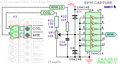
In the circuit C31, a 56 nF capacitor, is used as a high frequency bypass filter. The preset variable resistor VR1 works with the capacitor to form a kind of low pass RC filter. Protection diodes D7 & D8 are designed to prevent damage to the IC. U9 is a Schmitt trigger (six inputs) but only one input is actually used! It should be carefully noted that case's end connector Y2-pin 4, which was also used for the original 2A0 and 2A1 controllers, may be printed with the words RPM. The only RPM inputs are actually on Y3 (side of the case)as noted in the diagram, so if your end-plate does have RPM printed there, please remove it (as the input is actually grounded!). Monitoring High RPMs: C31 may be reduced in value to measure high RPMs. In operation, at high revs, C31 starts to act like a low value resistor, shunting the RPM signal to ground. If you find RPM signals start to go wrong at high revs, try changing C31 to say 560pF (100 times smaller!). Accuracy & Conversion: The M168 converts the RPM data into a count of 5 µSec time periods that is averaged over two successive RPM pulses. To convert this count to something useful, first assume we are looking at pulses from a 4 cylinder 4-stroke motor that produces two pulses per revolution (ie. PPR = 2.0). At 2,400 RPM there will be 2400/60 = 40 revs/sec or 80 pulses/sec. As each second is made up of 1,000,000/5 = 200,000 count periods, there will be a count of 200,000/80 = 2,500. So, a count of 2,500 corresponds to an RPM of 2,400. The generic formula is:
Higher revs produce smaller counts, and the lowest RPM that can be recorded (4 cyl., 4-stroke) for the 16 bit count field is 65,535 and this is 91.6 RPM - which is barely cranking speed for modern motors. At high RPM and high PPR rates the pulse frequency increases. The hardware low pass filter will start take effect at very high RPM and pulses will not be recorded accurately - in this case reducing C31's value may help (but possibly at the expense of more noise at lower RPMs). Quantisation Error: At high RPMs the lumpiness of the 5 µSec time intervals becomes apparent. At 8,000 RPM for a 4 cyl. engine (PPR = 2) the count will be 12,000,000/16,000 = 750. The next count, 751, would be recorded as an RPM of 12,000,000/(751*2) ≈ 7,989 RPM. So at 8,000 RPM the resolution is 11 RPM - at lower revs the resolution improves, and at higher PPR values (ie. for 6 and 8 cylinder engines) the resolution degrades. |
(7) Wideband Outputs - WBlin+/-, NBsim & SVout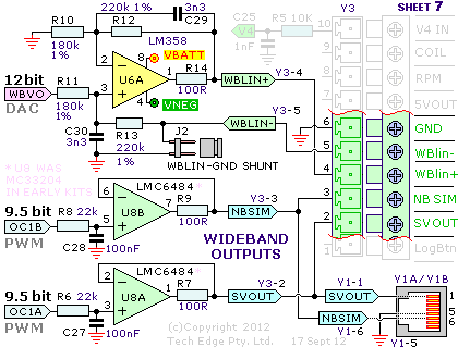
Three voltage outputs are provided. One high quality differential WBlin+/- output is generated on the lambda module by the 12 bit hardware DAC (WBVOUT circuit on Y7-p9). WBVOUT is amplified and filtered by U6A (LM358) and is output on the WBLIN+ line. The WBLIN- circuit is actually an input, and when the J2 shunt (WBLIN-GND) is OFF the WBLIN+ output will be lifted (or reduced) by the voltage on the WBLIN- input. We call this a differential output and the concept behind it is discussed further here. Just remember that if you leave WBlin- floating (not connected, or the WBLIN-GND shunt off) then the voltage on WBlin+ will be undefined - the best option is to leave off the WBLIN-GND shunt and connect WBlin- to the ground reference of your ECU, logger or target device that receives WBlin+. An important aspect of the differential WBlin driver circuitry is the negative bias voltage VNEG required to ensure WBlin+ can track both positive and negative changes on the WBlin- input (I'll say that again - WBlin- in an INPUT). This bias is obtained from the RS232 chip U5 described in the RS232 section. Note that WBlin- should not vary by more than +/- a few volts from the GND value (say +/- 3 Volts). If you leave WBlin- to float (ie. with the WBLIN-GND shunt removed) then WBlin+ could float up to VBatt, forcing WBlin+ to be at a considerably higher voltage than most devices connected to it will expect. Remember also, that to measure WBlin+ with a voltmeter, you should make sure the WBLIN-GND shunt is ON. The 12 bit DAC (DAC7612 on the lambda module), with an accurate internal reference, generates voltages in steps of exactly 1.0 mV. U6A is wired as a differential amplifier with bias correction and has a gain of 220/180) and gives WBlin a maximum value of 4.095*220/180 = 5.005 Volts in steps of ≈1.22 mVolts. Note the 100 Ohm resistor R14 is used to limit short circuit output current and is wired in the feedback loop to avoid changes in the output voltage when low impedance loads are used. The CPU's OC1A & OC1B outputs are set up as two 10 bit PWM generators. A simple single pole filter, using op-amp sections U8A & U8B adds some smoothing and filtering to each output. In practise this results in the SVout and NBsim signals having somewhat less than the 10 bits of PWM resolution available, so we have called each PWM circuit a 9.5 bit DAC. All outputs are available on pluggable connector Y3. The single ended outputs NBSIM and SVOUT (along with GROUND) are also available on Y1A & Y1B (but note that Y1A/Y1B includes other circuits not shown on this schematic). |
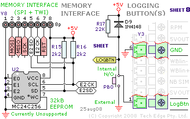
(8) Interface (TWI + SPI) & On-Board Logging Button(s)
The on-board memory is used to store data when on-board logging is active. The two 2.2 k resistor are the required pullup for the TWI SCL and SDA lines. A 100,000 programing cycle & 40 year data retention is claimed for the device. On-board logging is controlled by press-button switch PB0 (refer to logger details here). Components R17 and D9 interface the switch to the processor and provide a small amount of protection for the mux U3 (not shown) that the LOGBTN signal connects to. |
(9) 1 Megabyte Flash Logger Module
The logger circuit, which uses a 3.3 Volt SST flash part U602, must be interfaced to the microcontroller's 5 Volt bus. The two HC single gate buffers (U603 & U604) and an HCT gate (U605) Provide two-way level conversion for the SPI Signals. This scheme ensures reliable high speed operation as compared to a simpler scheme using resistors. The U606 NE555 pulse/timer device, wired as a monostable, provides pulse extension of the Data ENable (DEN) signal so operation of the module can be seen as a flashing of the surface mount LED D1. Note the E2CK signal, as defined on the logger module, changes to DEN (Data ENable) and E2SD changes to LCH (LatCH). This is to more correctly identify the TWI lines as being used in a simple bit toggle mode.
|
(A) Power and Status LEDs & External 5 volt Power Supply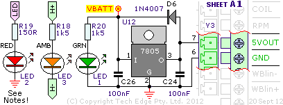
2Y2 has a low current regulated 5 Volt supply that can be used for sensors (like MAP, TPS, etc.) or other purposes outside the 2Y2. The regulator U12 operates like, and is physically attached like the main regulator U10 and also use VBATT as its input. Only limited heat sinking is available on the main board so keep current drawn from this regulator to 200mA or less (although a larger current can be handled by the regulator, it will thermally limit if overloaded, so check the actual output voltage if you find this part getting warm (it is the regulator closest to the CPU, ie. on the left under the lambda module). Capacitors C24 and C26 provide filtering to the regulator and diode D6 provides protection if VBATT should be shorted out. The regulator itself provides both thermal overload and output short circuit protection. The three indicator LEDs along with current limiting resistors R18, R19 & R20 are mounted between the logging button and the green connector Y3 (on the side). Green LED1 : (also called GRN) is a simple power monitor and should always be lit when unregulated power is supplied to the unit. Note that it will NOT show a failure of the main regulator U10. Amber LED3 : (also called AMB) shows the average power level supplied to the lambda sensor's heater circuitry and may have a just-perceptible flicker in normal operation - if there is a heater open circuit (or no sensor connected) it will flash sharply but at a much slower than normal rate (and the red status LED will show additional information). |
(B) RS232 Driver, Splitter, (-)ve Generator, Y1A & Y1B
A special adaptor cable is required for adapting the RJ45 connector's RS232 and power signals for connecting the unit to a PC, display, or logging device (see RS232 Data Cable below). The DBATT point provides connected devices with a current limited source of power and is used by various displays. Note: as the current is limited by a 3.3 Ohm resistor, a short across DBATT to GND will result in up to 4 Amps of current - this will be enough to cause the 1 Watt resistor R2 (dissipating 50 Watts) to overheat in a few seconds. This short-circuit current may not be enough current to blow the internal 3 Amp fuse but it may be enough to eventually vapourise the PCB's track to R2, or simply enough to char the paint on R2 - If you have an external display that doesn't seem to be working, then make sure R2 has not been overheated (as this can change it value and lower the available voltage to the external display) Y1A & Y1B also brings out the NBSIM & SVOUT analog signals (SVout is for compatibility with older displays like the LD01 and TE-5301, but note that the TE-5301 has a DB9 connector, and will note mate directly with Y1). |
(C) Sensor Cables (7200/07057, 6066, 17025 & L1H1)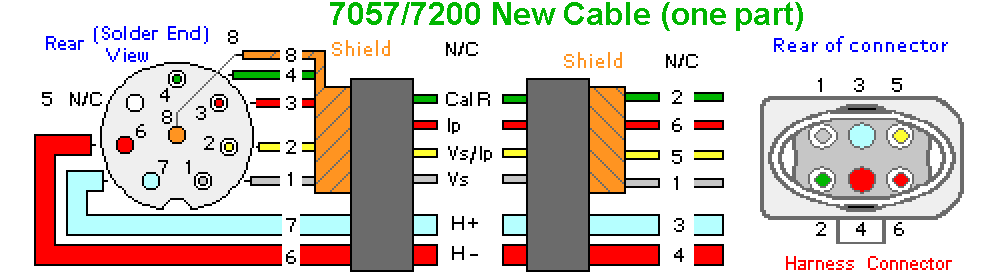
This cable connects the wideband unit to the sensor. Specifically, the cable is from 2Y's circular 8 pin connector (Y5) to the sensor. The schematic shown is for the 7200/7057 sensor. Also available are very detailed schematics and images of other WBo2 cables. Shown here is a 7200/7057 connector with attached cable. Here is the main cable construction page and much information about the actual connectors is on this page |
(D) Serial (RS232) Cable = WB-PC cable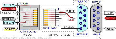
The serial (or RS232) data cable is an external cable that plugs in to one of the two RJ45 connectors (Y1A or Y1B) at the side and sensor/power connector end of the 2Y2 unit. The cable has two wires and a shield that acts as a third common wire. Here's an image of the RJ45 end of the cable and detail of just the DB9 end of the cable. In the above image the RJ45 socket (left) is on the 2Y2 unit, the rightmost male DB9-P (plug) is the connector at the back of a PC. Remember that the face of all DB9 connectors carries the pin numbers (so you don't have to guess). The DB9-S (socket) is the female end which is on the cable itself. The clear RJ45 crimp-connector is the same plug used for Ethernet cables and can be crimped with the same tool. In the schematic above:
Here's what's in the DB9 connector kit which is available as spare part [DB9FKIT]. Pre-built RS232 cables (1.2 m long) are available as spare part [12RS232]. For PDA use (ie. Palm, etc.) a different cable connection is required. Refer to the Palm Logging page for more information. |
(E) Four Digit 7-Segment Display Option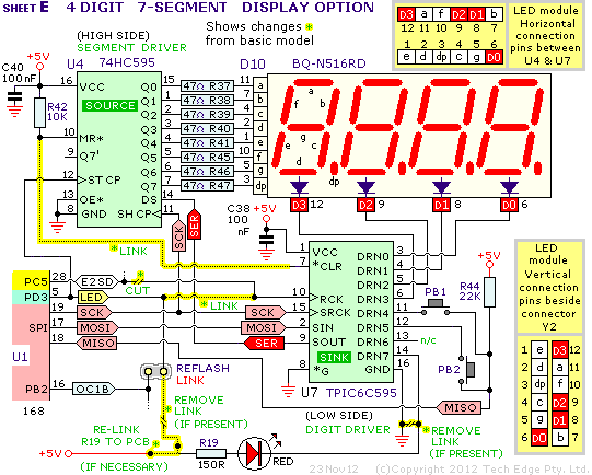
The Display on the 2Y2 comes as an optional set of additional parts. The original 2Y1 had a display area on the PCB, but because we couldn't source a part (TB62710 in DIP format) we decided to make small changes to the board to use a generic 74HC part that performed much the same function. We also fixed smalls errors on the PC - but as is usually the case, the first rev of the 2Y2 board has its own errors, and we changed our mind about how to drive the status LED & LED display after we had the boards made (see below for more info) - this means small changes to the 2Y2 PCB must be made to get the Red status LED working when the 7-segment display is NOT installed, and other changes made when the display is installed. The four-digit 7-segment common cathode display module D10 (BQ-N516RD) is driven by high side (ie. from 5 Volts) 7-segment driver U4 (74HC595) and low side (ie. to GND) digit driver U7 (TPIC6C595). Four additional outputs from the digit driver allow the status LED to be driven and two push buttons to be sensed (using MISO). The status LED drive pin from the CPU (LED) is used to control the loading and storing of serial data into U4 & U7 - when the display is not present (and after reconfiguring the wiring) the LED signal drives the status LED directly. 2Y2 Updates (Nov 2012)The PCB, as supplied, is configured to control the display using one of the TWI (or I2C) signals (E2SD). This is a problem becasue it means the on-board logging memory, that also uses these signals, would not be usable with the display. So we have to make changes to the 2Y2 PCB so logging memory and the display can co-exist. This change also requires us to have a display and non-display firmware (ie. HXF file) version for each of the sensors (LSU-4.2 & LSU-4.9) supported. With the modifications outlined here this is how the 2Y2 drives the display: The display driver chips high-side and low-side signals are controlled by the processor's SPI lines (MOSI & SCK) and the PD3 (LED) line previously used to drive the Red LED directly. The SPI (Serial Peripheral Interface) lines serially clock data into both driver chips (as a 16 bit word), U4 receives its serial data from U1 via U7on the SER line - this scheme allows a single data stream (from the M168's MOSI) to filter through both chips (so in theory, U4's Q7* output could be cascaded to another chip if we wanted to expand the display). The PD3 are also used in bit set/clear mode to transfer the latched data to the driver chips' outputs. Low side driver U7 is a very high current HexFET switch and is set to sequentially select outputs DRN0 to DRN3 that drive each of the 4 digits. Only one digit is selected at one time and very little power is dissipated by the low side driver due to its low ON impedance. High side driver U4 drives the digit's segments (a through g & dp). The LED current is controlled primarily by the high side driver's internal impedance and by the eight 47 ohm current limiting resistors R37, R38, R39, R40, R41 & R45, R46, R47. The display's apparent brightness is varied in firmware by controlling how long the digits are enabled for.Other components on the schematic are R42 a pull-up for U4 (and U7 when the required modification is made) and R44 a pull-up for sensing the optional push-buttons PB1 & PB2. R19 and RED (the status LED parts) have been described above and in this section. On the 2Y2 board the low side output DRN6 is unused. Also shown on the schematic are the two connection points for the LED module's pins that are in a 6 x 2 row format. The top right (larger) diagram shows the connection points when the LED module is used flush with the top surface of the case. The lower right diagram is when the module is used at the left end of the case (in place of Y2). Refer to further construction information on how best to mount the LED display as there are several possible ways to do it, and no one way is considered correct. |
We appreciate your feedback on the content and any corrections necessary to this document.
 The M168 has only small amounts of non-volatile memory but external memory (called on-board logging memory)
can be used to store AFR and other data sensed through the input channels.
There are two memory interface busses
The M168 has only small amounts of non-volatile memory but external memory (called on-board logging memory)
can be used to store AFR and other data sensed through the input channels.
There are two memory interface busses 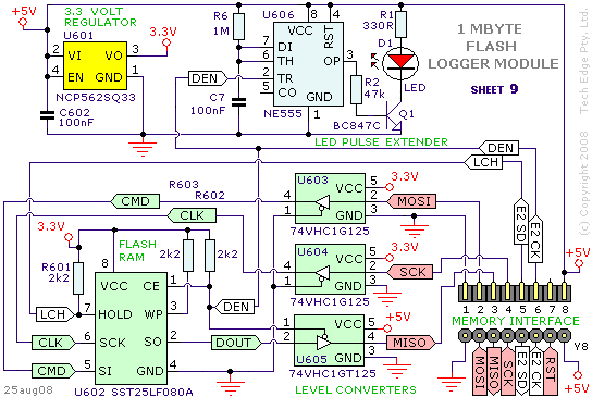 The 1 Mbyte Flash
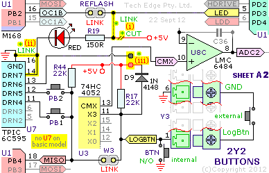
 For the in-built display version, the status LED is driven differently!
The 2Y2 PCB requires small modifications and this section highlights the changes for the non-display version.
For the in-built display version, the status LED is driven differently!
The 2Y2 PCB requires small modifications and this section highlights the changes for the non-display version.
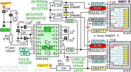 The serial driver chip U5 (HIN202, ST202, or equiv.) includes a charge pump circuit to produce a true negative RS232 rail.
This (-)ve voltage is also available externally (from U5-p6 V- pin)
and, after smoothing with capacitors C21, C17 & C18 and resistor R1 to create VNEG,
is used to generate a bias for the WBlin+/WBlin- driver circuit described above.
The serial driver chip U5 (HIN202, ST202, or equiv.) includes a charge pump circuit to produce a true negative RS232 rail.
This (-)ve voltage is also available externally (from U5-p6 V- pin)
and, after smoothing with capacitors C21, C17 & C18 and resistor R1 to create VNEG,
is used to generate a bias for the WBlin+/WBlin- driver circuit described above.
)
)
)
)
)
)
)
)
)
)
)
)